- 您现在的位置:买卖IC网 > Sheet目录369 > W948D2FBJX5E (Winbond Electronics)IC LPDDR SDRAM 256MBIT 90VFBGA
�� �
�
�W948D6FB� /� W948D2FB�
�256Mb� Mobile� LPDDR�
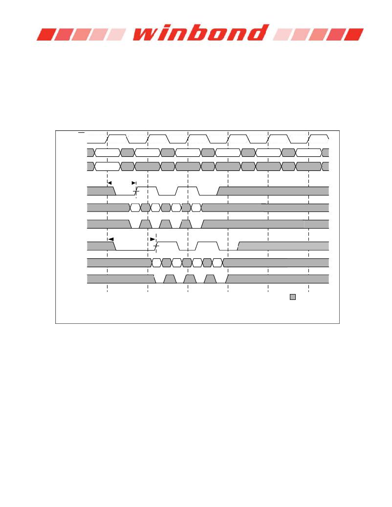
�7.6.3� Write� Burst� (min.� and� max.� tDQSS)�
�During� Write� bursts,� the� first� valid� data-in� element� will� be� registered� on� the� first� rising� edge� of� DQS� following� the�
�WRITE� command,� and� the� subsequent� data� elements� will� be� registered� on� successive� edges� of� DQS.� The� Low� state�
�of� DQS� between� the� WRITE� command� and� the� first� rising� edge� is� called� the� write� preamble,� and� the� Low� state� on�
�DQS� following� the� last� data-in� element� is� called� the� write� post-amble.�
�The� time� between� the� WRITE� command� and� the� first� corresponding� rising� edge� of� DQS� (t� DQSS� )� is� specified� with� a�
�relatively� wide� range� -� from� 75%� to� 125%� of� a� clock� cycle.� Following� figure� shows� the� two� extremes� of� t� DQSS� for� a�
�burst� of� 4,� upon� completion� of� a� burst,� assuming� no� other� commands� have� been� initiated,� the� DQs� will� remain� high-Z�
�and� any� additional� input� data� will� be� ignored.�
�CK�
�CK�
�Command�
�WRITE�
�NOP�
�NOP�
�NOP�
�NOP�
�NOP�
�Address�
�BA,Col� b�
�t� DQSSmin�
�DQS�
�DQ�
�DM�
�t� DQSSmax�
�DQS�
�DQ�
�DM�
�1)� DI� b� =� Data� In� to� column� b.�
�=� Don't� Care�
�2)� 3� subsequent� elements� of� Data� In� are� applied� i� nthe� programmed� order� following� DI� b.�
�3)� A� non-interrupted� burst� of� 4� is� shown.�
�4)� A10� is� LOW� with� the� WRITE� command� (Auto� Precharge� is� disabled)�
�7.6.4� Write� to� Write�
�Data� for� any� WRITE� burst� may� be� concatenated� with� or� truncated� with� a� subsequent� WRITE� command.� In� either�
�case,� a� continuous� flow� of� input� data,� can� be� maintained.� The� new� WRITE� command� can� be� issued� on� any� positive�
�edge� of� the� clock� following� the� previous� WRITE� command.�
�The� first� data-in� element� from� the� new� burst� is� applied� after� either� the� last� element� of� a� completed� burst� or� the� last�
�desired� data� element� of� a� longer� burst� which� is� being� truncated.� The� new� WRITE� command� should� be� issued� X�
�cycles� after� the� first� WRITE� command,� where� X� equals� the� number� of� desired� data-in� element� pairs.�
�Publication� Release� Date� :� Oct,� 15,� 2012�
�-� 35� -�
�Revision� :� A01-004�
�发布紧急采购,3分钟左右您将得到回复。
相关PDF资料
W949D2CBJX5E
IC LPDDR SDRAM 512MBIT 90VFBGA
W971GG6JB25I
IC DDR2 SDRAM 1GBIT 84WBGA
W971GG8JB-25
IC DDR2 SDRAM 1GBIT 60WBGA
W9725G6IB-25
IC DDR2-800 SDRAM 256MB 84-WBGA
W9725G6JB25I
IC DDR2 SDRAM 256MBIT 84WBGA
W9725G6KB-25I
IC DDR2 SDRAM 256MBIT 84WBGA
W972GG6JB-3I
IC DDR2 SDRAM 2GBITS 84WBGA
W9751G6IB-25
IC DDR2-800 SDRAM 512MB 84-WBGA
相关代理商/技术参数
W948D2FBJX5ETR
制造商:Winbond Electronics Corp 功能描述:256M MDDR, X32, 200MHZ
W948D2FBJX5I
制造商:Winbond Electronics Corp 功能描述:DRAM Chip DDR SDRAM 256M-Bit 8Mx32 1.8V 90-Pin VFBGA 制造商:Winbond Electronics Corp 功能描述:IC MEMORY
W948D2FBJX5I TR
制造商:Winbond Electronics Corp 功能描述:256M MDDR, X32, 200MHZ, INDUST
W948D2FBJX6E
制造商:Winbond Electronics Corp 功能描述:DRAM Chip DDR SDRAM 256M-Bit 8Mx32 1.8V 90-Pin VFBGA 制造商:Winbond Electronics 功能描述:LOW POWER DRAM 制造商:Winbond Electronics Corp 功能描述:IC MEMORY
W948D2FBJX6ETR
制造商:Winbond Electronics Corp 功能描述:256M MDDR, X32, 166MHZ, 65NM
W948D2FBJX6G
制造商:WINBOND 制造商全称:Winbond 功能描述:256Mb Mobile LPDDR
W948D6FB
制造商:WINBOND 制造商全称:Winbond 功能描述:256Mb Mobile LPDDR
W948D6FBHX5E
功能描述:IC LPDDR SDRAM 256MBIT 60VFBGA RoHS:是 类别:集成电路 (IC) >> 存储器 系列:- 标准包装:1 系列:- 格式 - 存储器:闪存 存储器类型:闪存 - NAND 存储容量:4G(256M x 16) 速度:- 接口:并联 电源电压:2.7 V ~ 3.6 V 工作温度:0°C ~ 70°C 封装/外壳:48-TFSOP(0.724",18.40mm 宽) 供应商设备封装:48-TSOP I 包装:Digi-Reel® 其它名称:557-1461-6